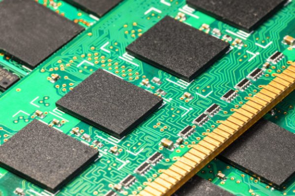

AI application chips are becoming more and more energy-consuming, imec application new technology reduces energy consumption impact
As global geopolitics and economic uncertainties are increasingly dramatic, innovation will be the key to driving economic prosperity, and artificial intelligence (AI) is the core force. However, the accelerated development of AI has led to a rapid growth in computing demand, accompanied by an explosive increase in energy consumption, which clearly becomes a key issue.
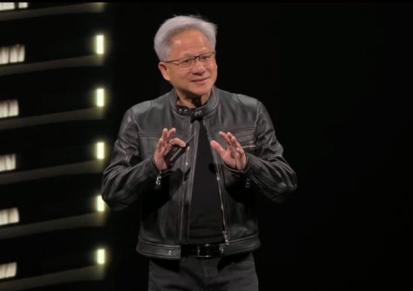
Although algorithmic innovation can reduce computing power demand, the efficiency of large language models to increase computing power and data is decreasing. Luc Van den hove, president and executive director of Belgium Microelectronic Research Center (imec), expected that AI will accelerate its popularity, especially in the future, more distinctive, proxy and physical AI wave will continue to promote the demand for large-scale computing capabilities, so it is important to improve computing energy efficiency.
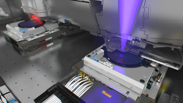
Luc Van den hove said in the 2025 Semicon Taiwan's master forum that the current semiconductor industry is focusing on the three core challenges of computing density, power management and memory bottlenecks, and proposes a series of breakthrough solutions. First of all, in terms of computing density, the extension of Morrow's law will rely on high-numeric pore ultraviolet (High-NA EUV) microfilm technology, which is expected to promote how much slimming will be achieved in the next twenty years. In order to reduce the speed of how much it is to reduce the speed, the industry actively utilizes 3D to stack transistors vertically through the CFET concept, as well as multi-layer chip stacking (CMOS 2.0), stack different functional wafer layers, each layer to optimize the process, greatly expand the CMOS route map. Finally, through 3D heterogeneous integration (advanced packaging), a computing unit larger than a single grain is constructed to comprehensively improve the computing density.
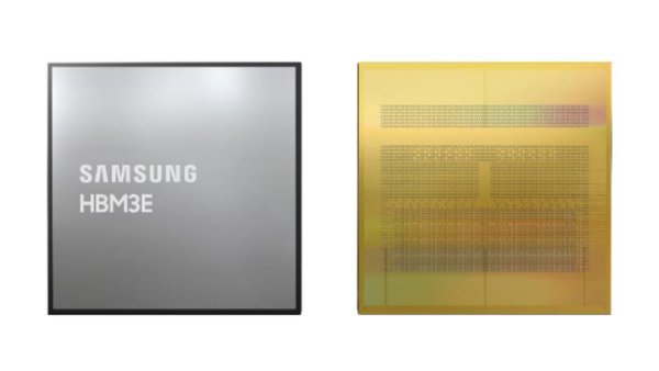
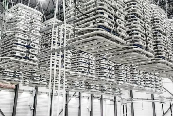
In addition, when breaking through the extreme limit of kilowatt-level power consumption, AI chips consume huge power, often exceeding kilowatts. Their power supply and heat dissipation, especially the hot point management in 3D stacking, is a huge challenge. Solutions include technical design optimization and direct liquid immersion cooling and other efficient heat dissipation technologies. As for reshaping data flow, AI chips spend most of their time and energy on data movement. Therefore, a large number of memory is integrated near the logical processing area, through 3D stacking, and new memory types such as vertical track memory chips are integrated. The system layer will optimize the memory level and integrate more computing units into the memory stack (AGM memory). Megabit connections between wafers will use co-packaged optical interconnects and active silicon photonic intermediary chips to greatly improve frequency width.
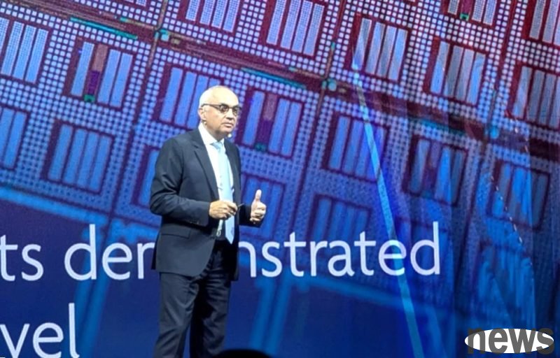
Luc Van den hove said that chip design is moving from traditional 2D to full 3D optimization, combining the concept of CMOS 2.0, it is expected to create a new architecture of software weight. This requires synchronous breakthroughs in algorithms, chip architecture and technical platforms, and strengthening the hardware software design. Among them, the concept of new computing has also made breakthroughs. Imec has demonstrated the scalability of ultra-guided low-temperature electronics, and is expected to reduce the entire data center by 2,000 times and reduce power consumption by 100 times. In terms of quantum computing, progress has been made in quantitative digit minification and integration, and a unique quantum backend architecture has been developed to lay the foundation for the realization of large-modulus qubit systems.
Luc Van den hove emphasizes that the current positive impact of AI has been shown in various fields. For example, in terms of health, imec uses nano and microfluidic technology to cultivate human blood and brain barriers on 3D chips, accurately test drugs, improve the treatment efficiency of brain diseases, and provide a model for AI drug discovery. In the mobile field, AI promotes automatic driving, imec is developing an efficient and reliable chip-level centralized computing platform to accelerate industry innovation through automatic driving chip planning.
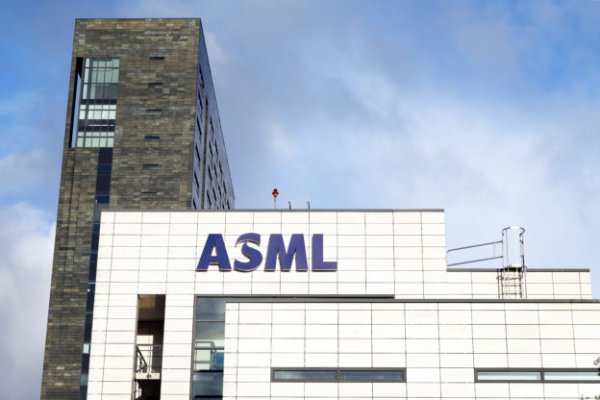
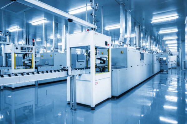
To support these breakthroughs, imec is carrying out large-scale R&D infrastructure expansion, investing 2.5 billion euros, doubling production capacity and adding 100 new cutting-edge equipment, including ASML's next-generation High-NA EUV machine. This expansion is supported by the European Commission, the CHIPS Act, the Denmark Government and industrial partners. Faced with challenges and opportunities in chip industry, the industry must embrace overwhelming innovation, priority cooperation, and promote openness and transparency, and jointly promote the full-speed transformation of the innovation engine in the AI era.