
Challenge Hyper-NA EUV? Scientists try new B-EUV micro-film and CLD sedimentation, which is expected to overwrite future chip manufacturing
Johns Hopkins University researchers reveal a new method of making chips, using lasers with wavelengths of 6.5 to 6.7 nanometers, or "Soft X-ray", which is expected to increase the resolution of exposure equipment to less than 5 nanometers.
According to the report of the foreign media "Cosmos", a journal of Nature Chemical Engineering, scientists call this method "B-EUV" (Beyond-EUV), meaning that this technology is expected to replace the current standard EUV micro-shading in the industry. But researchers also admitted that it took years to create experimental B-EUV equipment just to do it.
As for software X-rays, is there any chance to challenge the strongest Hyper-NA EUV at present? The report believes that theory is feasible.
The current EUV exposure manufacturing uses 13.5 nanometers in wavelength. As the wafer process continues to slightly shrink to 3 nm, 2 nm and even Ångström levels, the existing 0.33 NA EUV system (also considered as low-numeric pores [Low-NA EUV]) is also facing challenges due to a resolution of about 13.5 nm.
As for the High-NA EUV equipment of high-numerical pores, the resolution can be increased from 0.33 to 0.55, and the resolution can be increased to 8 nm, but when it is less than 1 nm, it must move towards Hyper-NA EUV. The goal is to push the numerical pores to 0.7~0.75, and the resolution can be increased to 4~5 nm.
However, this requires an extremely complex system design price, with advanced optical systems costing up to billions of dollars. ASML technology chief Martin van den Brink also admitted that the company is studying the feasibility of Hyper-NA technology, but has not made a final decision.
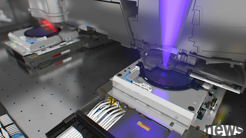
Johns Hopkins University team tried to break through Mor's law with "soft X-ray"The research team wrote in the article that although EUV with a wavelength of 13.5 nanometers has become the main candidate technology for less than 10 nanometers in semiconductor manufacturing, the next generation of microfilm tools are exploring shorter wavelengths, namely 6.x nanometers (6.5–6.7 nanometers) in the B-EUV range, to further break through the resolution limit.
In other words, the team intends to use shorter wavelengths and a medium-sized NA to achieve better resolution. However, B-EUV faces many challenges.
First, the light source is not yet mature, and it is currently incapable of production of 6.7 nanometers of radiation light. Although there are research teams who have tried to use ionic bodies such as Gadolinium laser generation, there is still a lack of reliable solutions.
Furthermore, because the short-wavelength photon energy of 6.5~6.7 nanometers has extremely high energy and poor interaction with traditional photoresist materials, it is difficult to apply it in actual application. Third, light with wavelengths of 6.5~6.7 nanometers will be absorbed and not reflected by all materials, so no multi-layer bulb film lenses for this type of radiation have been produced so far. Finally, there is a lack of an ecological system, and B-EUV exposure equipment needs to be designed from zero. Currently, related zero components and consumables (such as protective films pellicles and photomonitors The supply chain of photosks) does not exist.
To understand the challenges mentioned above, the Johns Hopkins team decided to start exploring specific metals to see how to improve the interaction of B-EUV (approximately 6 nanometer wavelengths) light and anti-irrigation materials in chip manufacturing.
The research team found that metals such as zinc can absorb B-EUV light and release electrons. These electrons then touch the organic compound "imidazoles" and react chemically with them, which can etch extremely detailed patterns on the crystal circle.
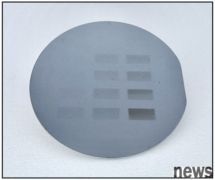
(Source: Johns Hopkins University)
Interestingly, although the galvanized does not perform well under traditional 13.5 nm EUV light, it is extremely effective at shorter wavelengths, and the importance of convex material matching with wavelengths.
In order to apply these metallic organic compounds to silicon wafers, researchers developed a "chemical liquid deposition" (simplified CLD) technology. This method can grow a film like a lens at a rate of 1 nanometer per second, with the film material "aZIF", amorphous zeolitic imidazolate frameworks.
In addition, CLD can also quickly test the combination between different metal and imidazoles, helping researchers to find the best matches suitable for different micro-film wavelengths. Research points out that although the galvanized is very suitable for B-EUV, other metals may perform better at different wavelengths, providing high flexibility for future wafer processes.
Researchers said this approach provides manufacturers with a "toolbox" covering at least 10 metal elements and hundreds of organic components to combine customized anti-magnetics for different microfilm platforms..
Although researchers have not solved all the challenges of B-EUV, they have found anti-agent materials that can be used with 6-nanometer wavelength light, created CLD processes, can lay uniform aZIF films on silicon wafers, and experimentally prove that metals such as gal can absorb soft X-rays and release electrons, and touch chemical reactions based on imidazole anti-agents. At present, B-EUV still has many challenges to be solved and cannot enter the mass production market. However, the report believes that the application range of CLD processes is quite wide and can not only be used in the semiconductor field, but also in non-semiconductor industries.
Researchers discover new methods for making smaller microchips Microchip manufacturing goes ‘beyond extreme’ with new technique ‘Beyond EUV’ chipmaking tech pushes Soft X-Ray lithography closer to challenging Hyper-NA EUV — ‘B-EUV’ uses new resistance chemistry to make smaller chips Extended reading: Exceeded expectations! AI chip new Groq raises US$750 million, with a valuation of US$69 billion We should challenge advanced technology of semiconductors and provide comprehensive solutions to four major materials.